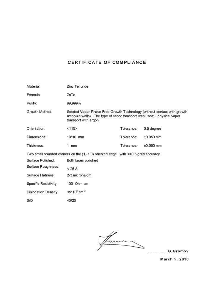
Halkogenidy A2B6 Single
MATERIALS FOR OPTOELECTRO
supplies A2B6 Single Crystal materials in ingots and wafers or other forms according to customers demands:
- Zinc Sulfide Cadmium Sulfide
- Zinc Selenide Cadmium Selenide
- Zinc Telluride Cadmium Sulphoselenide
Single crystals are grown by Seeded Vapor-Phase Free Growth Technology. The purity of the crystals is higher then 6N. By request, post growth annealing under Zn, Cd, S, Se partial pressure is provided to control of specific resistivity. Doping by In, Al, Cr, Fe, Ni and others impuritiesis also available.
BULK CRYSTALS
| Parameter | ZnS | ZnSe | ZnTe |
|---|---|---|---|
| Max. Ingot Sizes, mm | dia.- 40, height — 15 | dia.- 55, height — 15 | dia.- 40, height — 15 |
| Growth Direction | <111> | <111> or <100> | <111> |
| Structure | Cubic | Cubic | Cubic |
| Lattice Parameters, A | a=5.4093 | a=5.6687 | a=6.1034 |
| Specific Resistivity, Ohm x cm | |||
| undoped | 1×10⁸…1×10¹² | 1×10⁸…1×10¹² | 1…1×10⁶ |
| doped | — | 5×10⁻²…1×10⁶ | >108 |
| Hall Mobility, cm2/(V x sec) | 140 (e) | 400 (e) | 130 (h) |
| EPD, cm-2 | <5×10⁵ | 5×10³…1×10⁵ | <5×10⁵ |
| Density of low angle boundaries, cm-1 | — | <2 | <10 |
| Twins and stacking faults | <4% of hexagonal phase | twin free | twin free |
| Parameter | CdS | CdSe | CdSSe |
|---|---|---|---|
| Max. Ingot Sizes, mm | dia.- 50, height — 10 | dia.- 55, height — 15 | dia.- 40, height — 15 |
| Growth Direction | <0001> | <0001> | <0001> |
| Structure | Hexagonal | Hexagonal | Hexagonal |
| Lattice Parameters, A | a=4.1369 | a=4.2985 | 4.14<a<4.29 |
| c=6.7161 | c=7.0150 | 6.71<c<7.00 | |
| Specific Resistivity, Ohm x cm | 1…1×10¹⁰ | 1…1×10¹⁰ | 1…1×10⁸ |
| Hall Mobility, cm2/(V x sec) | 650 (e) | 1050 (e) | — |
| EPD, cm-2 | <5×10⁵ | <5×10⁵ | <5×10⁵ |
| Density of low angle boundaries, cm-1 | <50 | <50 | <100 |
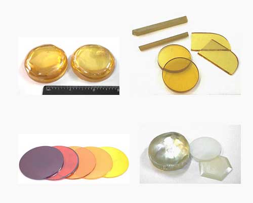
WAFERS
High quality single crystalline wafers are supplied in standard sizes: 5×5, 10×10 mm2 and dia. 25, 50 mm. Standardthickness is 1 mm. Other dimensions and shapes are available by request.
MAXIMAL DIMENSIONS OF WAFERS (in mm)
| Orientation | CdS | CdSe | CdSSe |
|---|---|---|---|
| <0001> | dia. 50 | dia. 50 | dia. 50 |
| <10-10> | 45×15 | 45×15 | 45×15 |
| <11-20> | 45×15 | 45×15 | 45×15 |
| Orientation | ZnS | ZnSe | ZnTe |
| <111> | dia. 40 | dia. 55 | dia. 40 |
| <110> | 35×20 | 40×20 | 35×15 |
| <100> | 20×20 | dia. 40 | 25×15 |
*- at thickness 1 mm
SURFACE FINISH
As-cut
OpticalPolishing
STANDARD ORIENTATION
<100>, <110>, <111> ±30 arc minutes for cubic crystals.
<0001>, <10-10>, <11-20>±30 arc minutes for hexagonal crystals.
Other orientations available on request.
TOLERANCES
Width/Length, mm ±0.050
Diameter, mm +0.000/-0.10
Thickness, mm ±0.050
APPLICATIONS
ZnS -UV-radiation semiconductor lasers for optical lithography;
ZnSe — blue radiation semiconductor lasers for projection systems:
substrates for epitaxy
electric field gauge
IR-opticalelements
light modulators
ZnTe — green radiation semiconductor lasers for projection systems
terahertz sensors and lasers
substrates for epitaxy;
CdS, CdSe — optical elements;
Zn1-xCdxSe — light-blue and red radiation semiconductor lasers for projection systems;
Zn1-xCdxS Zn1-xCdxS — light-blue and red radiation semiconductor lasers for projection systems;
ZnS1-xSex — UV-radiation semiconductor lasers for optical lithography;
ZnS1-xTex — cathode luminescent single crystal screen for high resolution projection systems;
CdS1-xTex -cathode luminescent single crystal screen for high resolution projection systems;